- 您现在的位置:买卖IC网 > Sheet目录3841 > PIC16F737-I/SP (Microchip Technology)IC PIC MCU FLASH 4KX14 28DIP
PIC16F7X7
DS30498C-page 42
2004 Microchip Technology Inc.
4.7.2
SEC_RUN MODE
The core and peripherals can be configured to be
clocked by T1OSC using a 32.768 kHz crystal. The
crystal must be connected to the T1OSO and T1OSI
pins. This is the same configuration as the low-power
timer circuit (see Section 7.6 “Timer1 Oscillator”).
When SCS bits are configured to run from T1OSC, a
clock transition is generated. It will clear the OSTS bit,
switch the system clock from either the primary system
clock or INTRC, depending on the value of SCS<1:0>
and FOSC<2:0>, to the external low-power Timer1
oscillator input (T1OSC) and shut-down the primary
system clock to conserve power.
After a clock switch has been executed, the internal Q
clocks are held in the Q1 state until eight falling edge
clocks are counted on the T1OSC. After the eight clock
periods have transpired, the clock input to the Q clocks
is released and operation resumes (see Figure 4-8). In
addition, T1RUN (in T1CON) is set to indicate that
T1OSC is being used as the system clock.
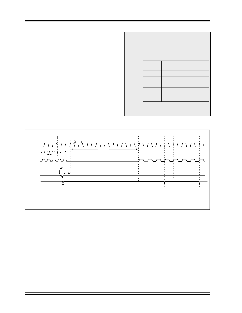
FIGURE 4-8:
TIMING DIAGRAM FOR SWITCHING TO SEC_RUN MODE
Note 1: The T1OSCEN bit must be enabled and it
is the user’s responsibility to ensure
T1OSC is stable before clock switching to
the T1OSC input clock can occur.
2: When T1OSCEN = 0, the following
possible effects result.
Original
SCS<1:0>
Modified
SCS<1:0>
Final
SCS<1:0>
00
01
00
– no change
00
11
10
– INTRC
10
11
10
– no change
10
01
00
– Oscillator
defined by
FOSC<2:0>
A clock switching event will occur if the
final state of the SCS bits is different from
the original.
Q4
Q3
Q2
OSC1
SCS<1:0>
Program
PC + 1
PC
Note 1:
TT1P = 30.52
s.
2:
TOSC = 50 ns minimum.
3:
TSCS = 8 TT1P
4:
TDLY = 1 TT1P.
Q1
T1OSI
Q1
TSCS(3)
Counter
Q1
TT1P(1)
System
Clock
TOSC(2)
Q3
Q2
Q4
Q1
Q2
PC + 2
PC + 3
Q3
Q4
Q1
TDLY(4)
发布紧急采购,3分钟左右您将得到回复。
相关PDF资料
PIC18F86K22-I/PTRSL
MCU PIC 64K FLASH XLP 80TQFP
PIC16C63A-04I/SP
IC MCU OTP 4KX14 PWM 28DIP
PIC16C63A-04I/SO
IC MCU OTP 4KX14 PWM 28SOIC
52559-2270
CONN FFC 22POS .5MM VERT ZIF SMD
52559-1870
CONN FFC 18POS .5MM VERT ZIF SMD
DSPIC33EP64MC506-I/PT
IC DSC 16BIT 64KB FLASH 64TQFP
52745-1896
CONN FFC 18POS .5MM R/A ZIF SMD
PIC16LC622-04/P
IC MCU OTP 2KX14 COMP 18DIP
相关代理商/技术参数
PIC16F737-I/SP
制造商:Microchip Technology Inc 功能描述:IC 8BIT FLASH MCU 16F737 SDIL28
PIC16F737-I/SS
功能描述:8位微控制器 -MCU 7KB 368 RAM 25 I/O RoHS:否 制造商:Silicon Labs 核心:8051 处理器系列:C8051F39x 数据总线宽度:8 bit 最大时钟频率:50 MHz 程序存储器大小:16 KB 数据 RAM 大小:1 KB 片上 ADC:Yes 工作电源电压:1.8 V to 3.6 V 工作温度范围:- 40 C to + 105 C 封装 / 箱体:QFN-20 安装风格:SMD/SMT
PIC16F737T-I/ML
功能描述:8位微控制器 -MCU 7KB 368 RAM 25 I/O RoHS:否 制造商:Silicon Labs 核心:8051 处理器系列:C8051F39x 数据总线宽度:8 bit 最大时钟频率:50 MHz 程序存储器大小:16 KB 数据 RAM 大小:1 KB 片上 ADC:Yes 工作电源电压:1.8 V to 3.6 V 工作温度范围:- 40 C to + 105 C 封装 / 箱体:QFN-20 安装风格:SMD/SMT
PIC16F737T-I/SO
功能描述:8位微控制器 -MCU 7KB 368 RAM 25 I/O RoHS:否 制造商:Silicon Labs 核心:8051 处理器系列:C8051F39x 数据总线宽度:8 bit 最大时钟频率:50 MHz 程序存储器大小:16 KB 数据 RAM 大小:1 KB 片上 ADC:Yes 工作电源电压:1.8 V to 3.6 V 工作温度范围:- 40 C to + 105 C 封装 / 箱体:QFN-20 安装风格:SMD/SMT
PIC16F737T-I/SS
功能描述:8位微控制器 -MCU 7KB 368 RAM 25 I/O RoHS:否 制造商:Silicon Labs 核心:8051 处理器系列:C8051F39x 数据总线宽度:8 bit 最大时钟频率:50 MHz 程序存储器大小:16 KB 数据 RAM 大小:1 KB 片上 ADC:Yes 工作电源电压:1.8 V to 3.6 V 工作温度范围:- 40 C to + 105 C 封装 / 箱体:QFN-20 安装风格:SMD/SMT
PIC16F73-E/ML
功能描述:8位微控制器 -MCU 7 KB 368 RAM 25I/O RoHS:否 制造商:Silicon Labs 核心:8051 处理器系列:C8051F39x 数据总线宽度:8 bit 最大时钟频率:50 MHz 程序存储器大小:16 KB 数据 RAM 大小:1 KB 片上 ADC:Yes 工作电源电压:1.8 V to 3.6 V 工作温度范围:- 40 C to + 105 C 封装 / 箱体:QFN-20 安装风格:SMD/SMT
PIC16F73-E/SO
功能描述:8位微控制器 -MCU 7KB 192 RAM 22 I/O RoHS:否 制造商:Silicon Labs 核心:8051 处理器系列:C8051F39x 数据总线宽度:8 bit 最大时钟频率:50 MHz 程序存储器大小:16 KB 数据 RAM 大小:1 KB 片上 ADC:Yes 工作电源电压:1.8 V to 3.6 V 工作温度范围:- 40 C to + 105 C 封装 / 箱体:QFN-20 安装风格:SMD/SMT
PIC16F73-E/SP
功能描述:8位微控制器 -MCU 7KB 192 RAM 22 I/O RoHS:否 制造商:Silicon Labs 核心:8051 处理器系列:C8051F39x 数据总线宽度:8 bit 最大时钟频率:50 MHz 程序存储器大小:16 KB 数据 RAM 大小:1 KB 片上 ADC:Yes 工作电源电压:1.8 V to 3.6 V 工作温度范围:- 40 C to + 105 C 封装 / 箱体:QFN-20 安装风格:SMD/SMT